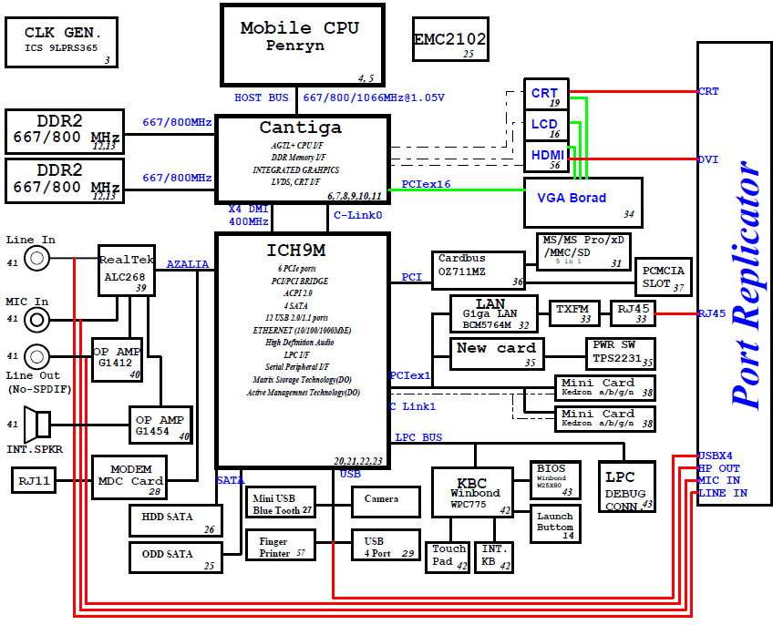
Acer Extensa 5630ZG (w/o 3G module), Motherboard schematic diagram Schematic diagram
|
|
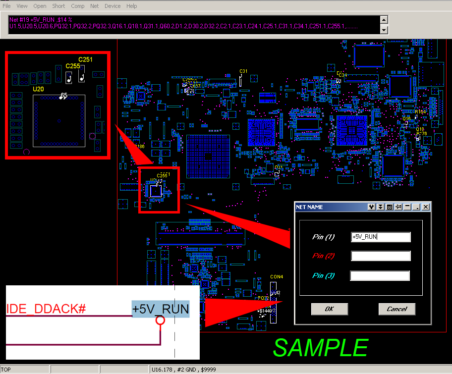
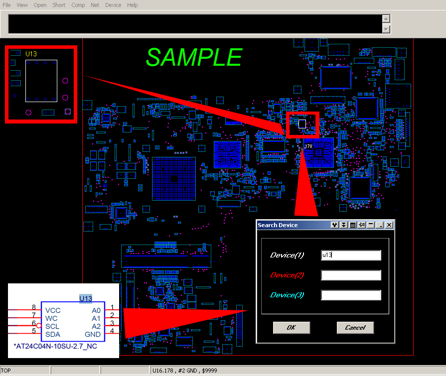
Price: US $15.00 **Power Block Diagram ***"Board view" file + software (viewer). Using this tool you will be able to find any component, pin or signal on your motherboard in a few seconds! *** All daughter board schematic diagrams, such as : Fingerprint module,Power Board,Touch Pad board, USB Board,Fingerprint Base board Major components CPU : Intel Penryn North Bridge : Cantiga South Bridge : ICH9M VGA : External MXM Clock Generator : ICS 9LPRS365 Audio Codec : ALC268 Audio Amplifier : G1412,G1454 KBC(Embeded Controller),SIO : Winbond WPC775 LAN Controller : BCM5764M CardBUS/1394/Cardreader Contr.: OZ711MZ Thermal Sensor : EMC2102 <Power System> TPS51125 TPS51124 TPS51100 G9131 APL5912 BQ24750 ISL6266A ISL6263 ! For models without 3G module only ::: PCB p/n: xx.4Z401.0xx ! Total Pages : 57 File tipe : PDF Language : English |
|---|